
The problem with traditional deposition
Semiconductor manufacturing has relied for decades on the same set of deposition technologies — PVD, CVD, and their many variants. These methods have been optimised to an extraordinary degree, but they share a fundamental constraint: as device geometries shrink and 3D architectures become the norm, achieving uniform, conformal coatings inside high-aspect-ratio features becomes exponentially harder. And more expensive.
The industry has pushed these tools to their physical limits. What was once a reliable process window is now a narrow corridor of parameters where even minor drift leads to yield loss. For advanced packaging, TSVs, and next-generation interconnects, the question is no longer how to optimise existing methods — it’s whether a different approach can deliver what they structurally cannot.
Why electrochemical deposition is different
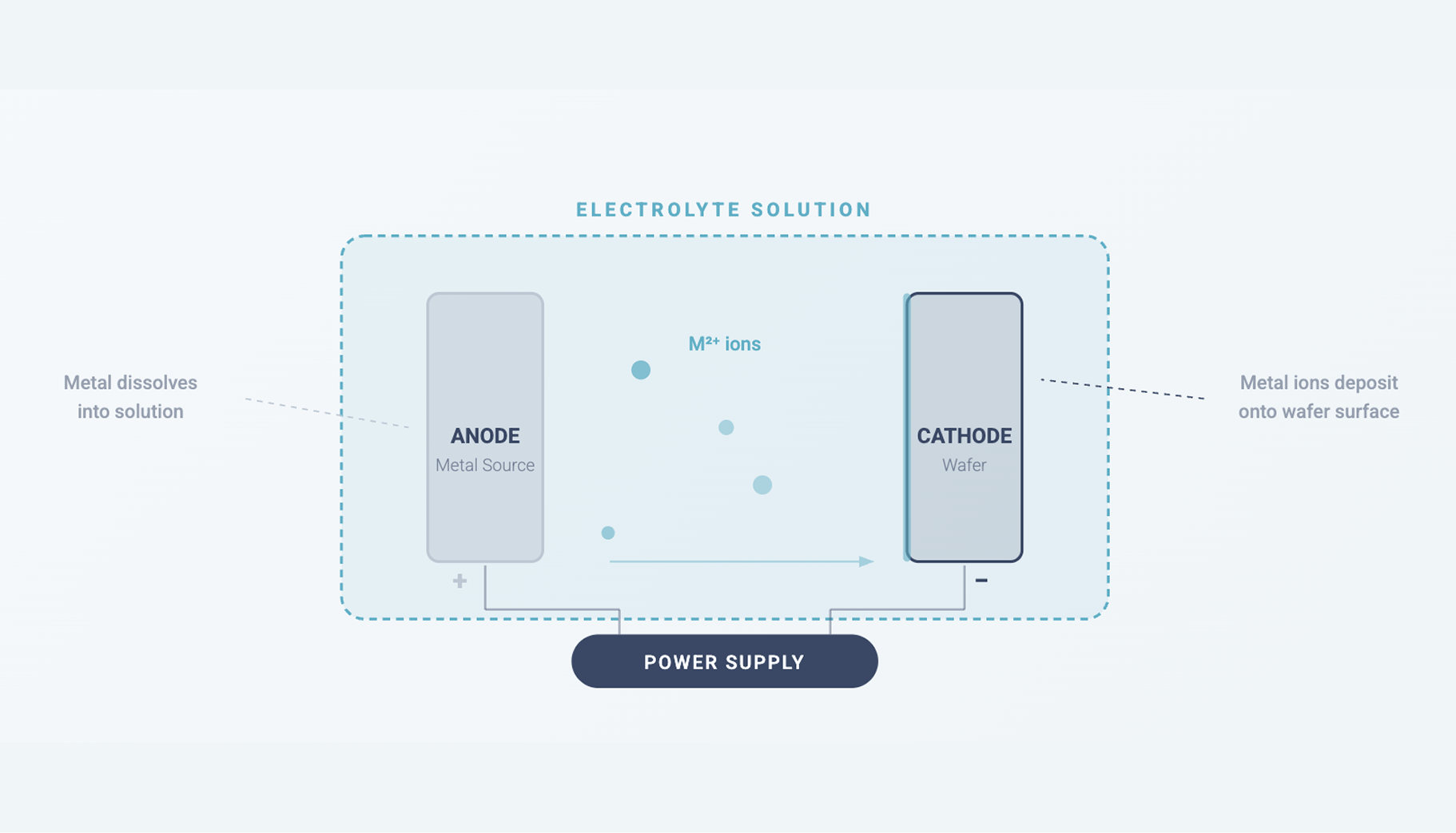
Electrochemical deposition — ECD — works on a fundamentally different principle. Instead of bombarding a surface with atoms in a vacuum chamber, it grows material from a liquid solution through a controlled electrochemical reaction. This isn’t new: ECD has been used in PCB manufacturing for decades. What is new is applying it with semiconductor-grade precision.
The advantages are rooted in physics. Because the process is driven by electric field distribution and solution chemistry rather than line-of-sight transport, ECD naturally fills features from the bottom up. This means conformal, void-free coatings even in aggressive geometries — something that PVD and CVD struggle with unless paired with complex multi-step sequences.
At Rise Technology, we’ve taken this principle and built an entirely new process architecture around it. Our approach controls deposition at the atomic level through proprietary electrolyte formulations, waveform engineering, and real-time process monitoring.
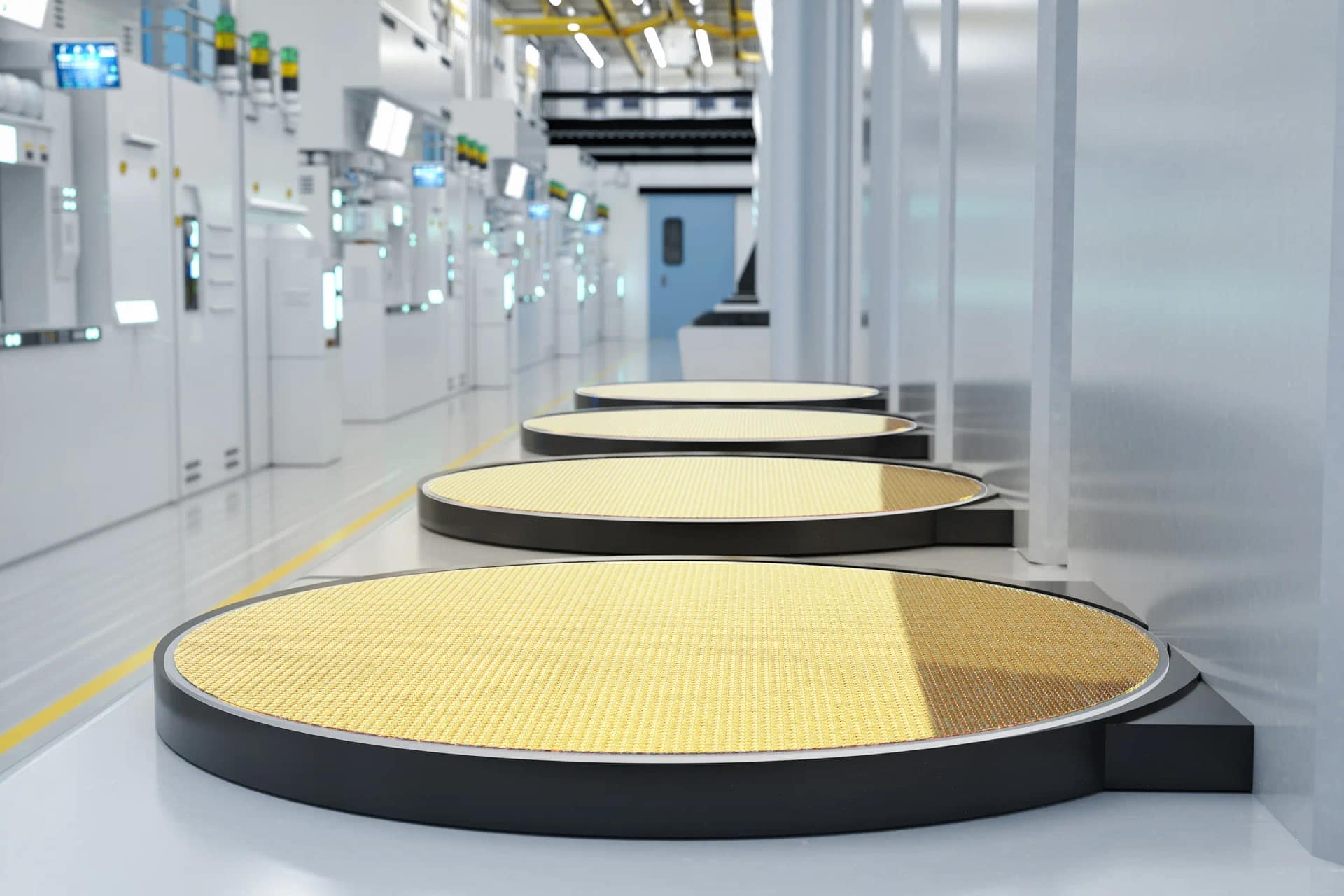
What happens inside our cleanroom
Our facility in Turin is where chemistry meets engineering. A typical process run starts long before any current flows.
First, the wafer is prepared through a cleaning and activation sequence tailored to the substrate material and target application. Then it enters our custom-designed ECD tool — built in-house by our equipment team — where it’s held in a precisely controlled electrolyte environment.
During deposition, we modulate current density, flow dynamics, and temperature in real time. Our monitoring systems track film growth as it happens, feeding data back into the process loop. The result is thickness uniformity and compositional control that meet semiconductor-grade specifications — consistently, wafer after wafer.
After deposition, every film goes through a characterisation pipeline: XRF for composition, profilometry for thickness mapping, SEM for morphology, and electrical testing where applicable. This feedback loop is what allows us to tighten process windows and move toward production-ready recipes.
From R&D to industrial reality
The gap between a working lab process and a production-worthy one is where most technologies stall. A beautiful film on one wafer means nothing if you can’t reproduce it on a thousand.
That’s why our roadmap has been production-oriented from day one. Every process we develop is designed with manufacturability in mind — defined process windows, statistical control limits, and equipment configurations that can scale. Our EIC Accelerator grant and CDP’s strategic investment are funding exactly this transition: from proven capability to industrial infrastructure.
We’re not trying to replace the entire deposition toolbox. We’re focused on the applications where ECD offers a step change — where conventional tools hit their ceiling and our approach unlocks performance, cost, or both.
What’s Next?
Over the coming months, we'll be sharing more about specific applications, technical results, and the milestones on our path to volume manufacturing. If you're working on advanced packaging, interconnects, or any application where deposition quality is the bottleneck, we'd like to hear from you.
Get in touch